America's Chip Dream Just Got Real: TSMC's Arizona Bet Pays Off
America's Chip Dream Just Got Real: TSMC's Arizona Bet Pays Off
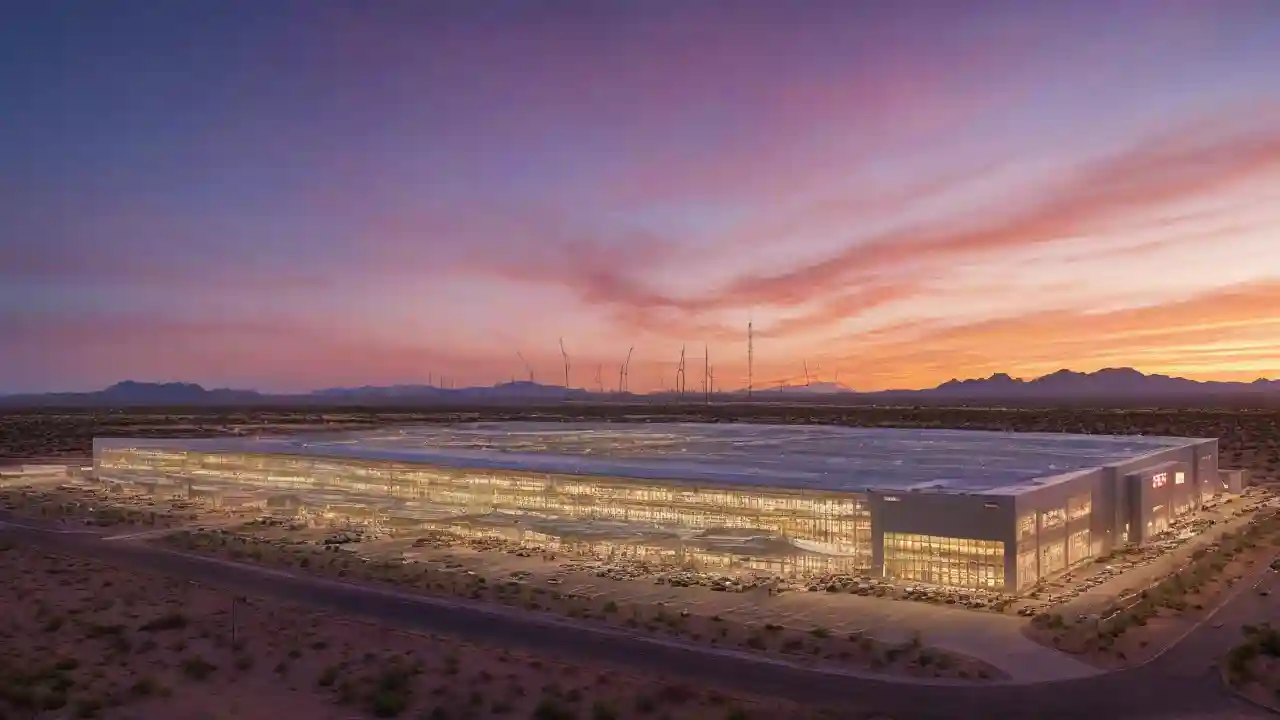
First US-made Nvidia Blackwell wafer rolls off Arizona production line as America races to break free from Taiwan's chipmaking stranglehold
PHOENIX — That silicon wafer rolling out of TSMC's Arizona plant this week? It's more than just another chip. It's proof that America's wildest industrial gamble since we split the atom might actually work.
We're talking about the first Nvidia Blackwell wafer made on US soil. The computational brain that'll power tomorrow's AI systems just became a little less dependent on a small island halfway around the world. TSMC's massive Phoenix "gigafab" has moved beyond speeches and ribbon-cuttings. They're making chips now. Real ones. Advanced ones.
The facility is already churning out 4-nanometer chips that match—sometimes beat—what comes out of Taiwan's best factories. After years of doubting whether cutting-edge chipmaking could even survive the trip to American soil, we've got our answer.
But here's the catch. That $165 billion sprawling across 1,100 acres of Arizona desert? It creates 20,000 solid jobs, sure. Yet critical pieces of the puzzle remain stubbornly Asian. Most advanced packaging—the delicate art of assembling multiple chiplets into finished processors—still happens over there. Even Arizona-born wafers must travel back across the Pacific for their final makeover.
The Timeline Just Got Crazy
TSMC's original schedule has been thrown out the window. The first fab hit high-volume production of 4-nanometer chips in late 2024. Ahead of schedule. The second facility was supposed to arrive in 2029 but now targets 3-nanometer production around 2028. Even wilder? They've already broken ground on facilities for 2-nanometer and advanced A16 chips. Industry watchers whisper these could be pumping out silicon by 2027—three years early.
One semiconductor analyst calls it "exponential demand meeting existential risk." AI chip shipments double every three months. Artificial intelligence products grabbed 57 percent of TSMC's third-quarter 2025 revenue of $33.1 billion. Meanwhile, smartphones' share dropped to 30 percent. TSMC projects AI accelerator demand will grow at mid-40 percent annually through 2029.
Taiwan's dominance creates what policymakers privately call "the trillion-dollar chokepoint." The island produces 90 percent of the world's advanced chips. One earthquake or military confrontation could crater the global economy by trillions. Rebuilding would take half a decade.
The Price of Coming Home
Here's where reality bites. US-produced chips cost more. AMD CEO Lisa Su and other industry sources indicate a 5 to 20 percent premium over Taiwanese equivalents. Labor costs more here. Infrastructure doesn't come cheap. Tariffs add up.
However, recent yield data tells a surprising story. TSMC's Arizona 4-nanometer facility achieves yields about 4 percentage points higher than comparable Taiwan operations during early runs. That's remarkable. Newer equipment helps. Stricter quality controls matter. Technical analysts estimate the real cost difference has shrunk to under 10 percent at full scale—way below the 30 to 50 percent premiums everyone feared initially.
For Nvidia and similar customers, pure cost isn't everything. Domestic production means insurance against export bans. Faster deliveries for US clients. A political story that opens doors with government and defense contractors. Hyperscalers like Microsoft and Google might swallow modest price bumps for supply chain security. When you're battling for AI infrastructure, a few extra percentage points don't matter much.
The Packaging Problem Nobody Wants to Talk About
Here's the asterisk on Arizona's triumph. Advanced packaging capacity remains mostly Asian. TSMC's Chip-on-Wafer-on-Substrate technology—essential for high-performance computing—has doubled to roughly 75,000 wafers monthly worldwide in 2025. But meaningful US packaging volume won't arrive before late 2027 or 2028.
Packaging specialist Amkor Technology plans an Arizona facility targeting early 2028. TSMC has announced intentions for on-site advanced packaging. Until then? Even Arizona-born wafers ship to Taiwan or elsewhere in Asia for final assembly. That undermines the whole resilience story that justified billions in federal subsidies.
"You're essentially building a sophisticated halfway house," notes one portfolio manager focused on semiconductor investments. "The wafer is American but the finished product still depends on Asian infrastructure. That's not independence. It's diversification with training wheels."
Desert Challenges: Water and Workers
Beyond geopolitics and economics lies something more mundane yet critical. Resource constraints. Each fab guzzles 2 to 3 million gallons of water daily. This region is already parched from decades of drought. TSMC promises 90 percent water recycling but local environmental groups remain skeptical about a six-fab cluster's cumulative impact.
Labor presents another headache. Semiconductor expertise takes years to develop. TSMC has leaned heavily on Taiwanese engineers and technicians to staff Arizona operations. Some industry estimates suggest US facilities lag Taiwan by several years in workforce maturity. That contributes to 30 percent higher labor costs that squeeze margins.
What This Means for Your Portfolio
Arizona's development crystallizes several tradeable themes for professional investors. Semiconductor equipment manufacturers stand to benefit big. Applied Materials, Lam Research, KLA Corporation—all gain from multiple waves of tool installations as additional fabs break ground and migrate to 3-nanometer and 2-nanometer processes. Inspection and metrology equipment demand intensifies at advanced nodes. That creates durable revenue streams.
Nvidia remains the most direct play on AI infrastructure buildout. Arizona production reduces geopolitical risk premiums while maintaining pricing power through 2026. Watch for any concrete commitments on US advanced packaging capacity allocation. Packaging bottlenecks represent the primary constraint on near-term supply expansion.
TSMC itself presents compelling risk-reward dynamics. Arizona has transformed from corporate responsibility expense to strategic asset. The company's ability to achieve sub-10 percent cost premiums while securing $6.6 billion in federal grants and loans materially improves return calculations. Key risks? Water permit challenges, skilled labor shortages, packaging localization delays that could push "Arizona-to-system" timelines beyond 2028.
Market observers suggest tactical positions in packaging specialists with US facility plans while hedging timeline uncertainty around environmental regulatory milestones. The gap between wafer production and finished systems represents both narrative vulnerability and opportunity as infrastructure gaps close.
Investment Disclaimer: This analysis reflects market conditions and established economic patterns as of October 2025. Semiconductor investments carry significant volatility related to technological shifts, geopolitical developments, and cyclical demand patterns. Past performance doesn't guarantee future results. Consult qualified financial advisors before making investment decisions and conduct independent due diligence on specific securities.
The Real Question: Victory or Expensive Insurance?
TSMC's Arizona gigafab has progressed from political symbolism to manufacturing substance. But the journey from first wafer to full supply chain sovereignty stretches years ahead. The 3-nanometer production targeted for 2028 will mark genuine leading-edge domestic capacity. Meanwhile, 2-nanometer and A16 processes look like end-of-decade achievements with potential for modest acceleration.
The fundamental question transcends manufacturing timelines. Can the United States build not merely fabs but a complete semiconductor ecosystem? One including packaging, materials, and specialized talent? The answer determines whether Arizona represents America's silicon rebirth or an expensive hedge against a catastrophe that never arrives. A $165 billion insurance policy on the 21st century's most critical technology.
For now, that first Blackwell wafer stands as proof of concept. The industrial base is growing. The talent is arriving. The technology transfer is succeeding. Whether it arrives fast enough, complete enough, and cost-effectively enough to matter when the next crisis emerges? That remains the semiconductor industry's defining uncertainty.