
Bankrupt Chipmaker Wolfspeed Becomes First to Launch Commercial 200mm Silicon Carbide Wafers
Wolfspeed's 200mm Silicon Carbide Breakthrough: A Market-Shifting Materials Revolution
How a financially troubled semiconductor company just unlocked the economics of next-generation power electronics
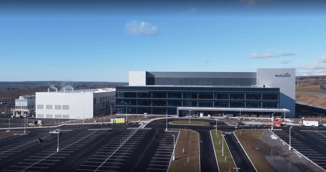
Wolfspeed Inc. has just delivered what industry analysts are calling a watershed moment. The Durham, North Carolina-based company announced Tuesday the commercial launch of its 200mm silicon carbide materials portfolio, marking the first time any supplier has brought industrial-scale SiC wafers of this size to market.

This isn't merely an incremental upgrade from the industry-standard 150mm wafers. The move represents a fundamental shift in the economics of power electronics manufacturing, potentially unlocking cost reductions of up to 54% for key components by 2030 while addressing critical supply bottlenecks that have constrained the electric vehicle and renewable energy sectors.
Silicon Carbide (SiC) is a compound semiconductor increasingly vital in power electronics. It outperforms traditional silicon, making it a superior choice for high-power, high-frequency applications.
Yet the announcement arrives with profound irony: Wolfspeed trades at just $1.47 per share, down 19% on Wednesday alone, having emerged from Chapter 11 bankruptcy restructuring mere days earlier. The company that may have just solved one of the semiconductor industry's most pressing scale challenges is itself fighting for survival.
The Scale Economics Revolution Behind the Numbers
The technical achievement extends far beyond diameter expansion. According to industry materials specialists, the transition from 150mm to 200mm wafers delivers approximately 1.78 times the surface area, translating to roughly 1.6 to 1.7 times more dies per wafer after accounting for edge losses and kerf effects.
Illustration showing the approximate increase in the number of semiconductor dies that can be produced from a 200mm wafer compared to a 150mm wafer.
| Wafer Characteristic | 150mm Wafer | 200mm Wafer | Increase (200mm vs 150mm) |
|---|---|---|---|
| Diameter | 150 mm | 200 mm | — |
| Approximate Surface Area | ~17,671 mm² | ~31,416 mm² | ~78% |
| Approximate Number of Dies | Base Line | ~1.85x | ~85% |
More critically, Wolfspeed's 200mm wafers feature enhanced parametric specifications at 350µm thickness with what the company terms "industry-leading doping and thickness uniformity." This uniformity directly impacts MOSFET yields—the percentage of functional chips produced per wafer—which represents the primary cost driver in SiC device manufacturing.
Dr. Cengiz Balkas, Wolfspeed's Chief Business Officer, emphasized that the launch "represents a materials innovation that empowers our customers to accelerate their device roadmaps with confidence." The company is positioning this not as a simple scaling exercise but as a quality breakthrough that enables next-generation high-voltage applications crucial for 800-1000V electric vehicle architectures.
The timing proves particularly strategic. Device manufacturers are establishing 200mm production lines throughout 2025-2026, creating immediate demand for compatible substrate materials. Wolfspeed's commercial availability addresses what industry experts describe as the "missing link" for Tier-1 suppliers planning large-scale platforms for 2026-2028 deployment.
Market Dynamics: A $10 Billion Prize Worth Fighting For
The broader silicon carbide semiconductor devices market, valued at approximately $1.52 billion in 2021, is projected to reach $10.39 billion by 2030, representing a compound annual growth rate exceeding 24%. Within this expansion, the SiC wafer segment alone is estimated at $2.27 billion in 2025, with 200mm wafers commanding premium pricing due to their scarcity and technical advantages.
Projected growth of the global silicon carbide (SiC) semiconductor device market from 2021 to 2030.
| Year | Market Size (USD Billion) |
|---|---|
| 2021 | 2.96 |
| 2024 | 5.23 |
| 2030 | 7.98 |
| CAGR (2022-2030) | 11.7% |
This growth trajectory is driven by urgent demand across multiple high-value sectors. Electric vehicle manufacturers require SiC components for more efficient powertrains and faster charging systems. Renewable energy installations depend on SiC-based inverters for improved grid integration. Industrial applications increasingly demand higher-performance power conversion solutions that only SiC materials can deliver at scale.
However, substrate availability has emerged as the primary bottleneck constraining market expansion. Traditional 150mm wafers, while mature, cannot deliver the cost structure necessary for mass-market SiC adoption. The economic advantages of 200mm substrates—combined with improved manufacturing yields—represent the key to unlocking broader industry transformation.
Current market intelligence suggests that quality 200mm SiC substrates command pricing above $2,000 per wafer, compared to Chinese 150mm alternatives that have fallen below $500. This pricing differential reflects not only the technical complexity but also the limited supplier base capable of delivering 200mm materials at commercial scale.
Competitive Battlefield: Racing Toward Industrial Supremacy
Wolfspeed currently maintains the strongest position in this emerging 200mm landscape, holding approximately 33-40% of the global SiC substrate market and operating the only fully integrated U.S. facility capable of commercial 200mm production at its Mohawk Valley fabrication plant.
Estimated global market share for silicon carbide (SiC) substrate manufacturers.
| Company | Market Share (%) | Year |
|---|---|---|
| Wolfspeed | 33.7 | 2024 |
| TanKeBlue | 17.3 | 2024 |
| SICC | 17.1 | 2024 |
However, the competitive environment is intensifying rapidly. STMicroelectronics is constructing a fully integrated 200mm SiC campus in Catania, with device production targeted for Q4 2025. Infineon Technologies is executing a phased 200mm ramp with volume production planned through FY25/26. ON Semiconductor is converting its Bucheon facility to 200mm production in 2025, leveraging its vertical integration from crystal growth through device manufacturing.
European competitors possess significant structural advantages, including established automotive relationships, long-term supply agreements, and substantial government support through various national semiconductor initiatives. These players are not merely following Wolfspeed's lead but developing parallel capabilities that could challenge its first-mover advantage within 12-18 months.
The most significant long-term threat emerges from Chinese manufacturers, including SICC, TanKeBlue, and Tianyue. These companies have rapidly gained market share through aggressive pricing strategies and are claiming 200mm readiness. While quality gaps remain, industry observers note these differentials are narrowing faster than many Western suppliers anticipated.
Financial Reality Check: Bankruptcy to Breakthrough
The contradiction between Wolfspeed's technical achievement and financial distress reflects the capital-intensive nature of advanced semiconductor manufacturing. The company recently completed Chapter 11 restructuring that reduced its debt burden from approximately $4.6 billion, providing greater operational flexibility. Support from Apollo Global Management and Renesas Electronics has stabilized the immediate financial outlook.
Yet execution risks remain substantial. Wolfspeed must simultaneously ramp production volumes, qualify materials with multiple customers across different applications, and maintain quality standards while facing intensifying price competition. The company's Siler City materials mega-fab, backed by CHIPS Act funding, represents a critical scaling milestone that must deliver on schedule to preserve market position.
Current trading at $1.47 per share reflects market skepticism about Wolfspeed's ability to capitalize on its technical advantages while managing financial constraints. The 37.8 million share trading volume on Wednesday—representing extraordinary retail and institutional interest—suggests investors are actively reassessing the company's prospects following the 200mm announcement.
Investment Implications: Positioning for the Power Electronics Revolution
For sophisticated investors, Wolfspeed's 200mm launch creates multiple strategic considerations. The company's technical leadership in a critical enabling technology offers significant upside potential if execution succeeds. The materials-first approach provides defensible competitive advantages that could compound over time as device manufacturers optimize designs around 200mm substrates.
However, the investment thesis faces headwinds from competitive dynamics and pricing pressure. Chinese substrate suppliers have demonstrated willingness to sacrifice margins for market share, potentially compressing Wolfspeed's premium pricing power. European competitors with stronger balance sheets and automotive relationships may capture high-value design wins in key growth segments.
Near-term catalysts include named customer wins for 200mm epitaxy supply agreements, automotive qualification milestones, and utilization metrics from both Mohawk Valley and the Siler City facility. Any disclosure regarding yield performance, defectivity rates, or gate oxide quality metrics would provide crucial visibility into commercial viability.
The broader investment opportunity extends beyond Wolfspeed to encompass the entire SiC value chain. Device manufacturers, module suppliers, and end-market applications from electric vehicles to renewable energy infrastructure may benefit from improved cost structures and performance characteristics enabled by 200mm substrates.
The Path Forward: Navigating Technical Excellence and Market Realities
Wolfspeed's 200mm silicon carbide launch represents a legitimate technical milestone that addresses urgent industry needs. The company has delivered commercial-scale materials that could unlock significant cost reductions and performance improvements across multiple high-growth applications.
Yet technical excellence alone cannot guarantee commercial success in the intensely competitive semiconductor industry. Wolfspeed must execute flawlessly on customer qualifications, production ramp schedules, and cost reduction initiatives while defending against well-funded competitors and aggressive pricing from alternative suppliers.
For the power electronics industry, the availability of commercial 200mm SiC materials marks an inflection point toward broader adoption across automotive, renewable energy, and industrial applications. The question is not whether 200mm substrates will become the industry standard—multiple suppliers are racing toward this goal—but rather which companies will capture value during this transition.
Wolfspeed has opened a crucial window of opportunity. Whether it can capitalize on this advantage while navigating financial constraints and competitive pressures will determine not only the company's future but also the pace of innovation across the broader power electronics ecosystem. For investors, the materials revolution in silicon carbide offers significant opportunities—but success will require careful evaluation of execution capabilities and competitive positioning rather than relying solely on technical achievements.
House Investment Thesis
| Aspect | Summary |
|---|---|
| Announcement | Wolfspeed's commercial launch of 200 mm SiC bare wafers and epitaxial wafers for immediate qualification. |
| Stock Context | WOLFSPEED, INC. (USA equity). Price: $1.47 USD (-$0.34). Open: $1.70. Volume: 37,795,320. High: $1.80, Low: $1.46. Trade Time: Thursday, September 11, 01:59:55 +0200. |
| Executive View | A real, commercial-scale milestone that addresses the SiC cost/capacity bottleneck. It's a materials scaling achievement, not new physics. Wolfspeed is the current leader, but competition is close and Chinese pricing is a risk. Company risk is lower post-Chapter 11 reorg but execution risk remains. |
| What's New | 350 µm 200 mm bare wafers and 200 mm epi wafers, emphasizing doping/thickness uniformity for MOSFET yield and faster time-to-market. |
| Significance | Area Scaling: ~1.6-1.7x more dies/wafer. Economics: Better capex per wafer-start and throughput per tool. Design: Enables higher-voltage, lower-Rds devices for 800-1000V EV and energy applications. |
| Problem Solved | Yes. Addresses supply, cost, and scale bottlenecks for 2026-28 platforms, countering Chinese price pressure on 150 mm. |
| Market Size | Devices TAM: ~$10-11B by 2030. Substrates/Epi TAM: ~$1-1.2B in 2024-25, growing mid-to-high teens. |
| Competitive Position | Wolfspeed: Materials leader (~33-40% share), only fully integrated US player with commercial 200mm. ST: Targeted 200mm device production Q4'25. Infineon/onsemi/Coherent: All ramping 200mm in 2025/26. China: Rapidly scaling with aggressive pricing, narrowing quality gap. |
| Unit Economics | Die Cost: Low-double-digit to ~25% reduction vs. 150mm. Wafer ASPs: Defensible margins near-term. Fab Throughput: Significant improvement in good-die per day. |
| Key Risks | 1. Execution & qualification cycles. 2. Pricing pressure from China. 3. Capex/Balance sheet discipline. 4. Reliance on non-US equipment vendors. |
| Who Benefits/Actions | Device Makers: Co-qual with Wolfspeed + backup, lock volume options. Auto OEM/Tier-1: Dual-source, insist on 200mm roadmaps. Renewables/Charging: Use for >250kW inverters/ >400kW chargers. Industrial/Data Center: Co-design for >98% efficiency. |
| Leading Indicators | Named customer wins/LT agreements, yield data (epi uniformity, defectivity), Mohawk Valley/Siler City utilization ramps, peer milestones (ST Q4'25, etc.). |
| Bottom Line | Excellent for buyers: Yes. Groundbreaking: Operationally yes, scientifically no. Solves urgent issue: Yes. Market big enough: Yes. Competitors: Everyone is racing to 200mm. Wolfspeed leading: On materials today, but lead is contested and depends on execution over next 4-6 quarters. |
Investment decisions should be based on comprehensive due diligence and individual risk tolerance. Past performance does not guarantee future results.