
SK Hynix Becomes First Company to Complete HBM4 Memory Chip Development and Prepare Mass Production for AI Systems
SK Hynix Breaks the Memory Wall: First HBM4 Chips Ready for AI's Next Battlefield
South Korean memory giant claims architectural breakthrough that could reshape datacenter economics as AI demand explodes
SK Hynix has completed development of the world's first HBM4 memory chips, marking a pivotal moment in the escalating race to feed artificial intelligence's insatiable appetite for data bandwidth. The announcement, made Wednesday from Seoul, positions the company to capture the lion's share of what industry analysts expect to be a $15+ billion market by 2030.
The breakthrough comes as AI datacenters strain under what engineers call the "memory wall"—a fundamental bottleneck where processing power vastly outpaces memory bandwidth. SK Hynix's HBM4 promises to shatter this constraint with a doubled bus width to 2,048 bits and operating speeds exceeding 10 gigabits per second, delivering bandwidth improvements that could boost AI service performance by up to 69%.
The "Memory Wall" describes a fundamental bottleneck in computer architecture, representing the widening performance gap between increasingly fast processors and much slower memory access times. This disparity means CPUs frequently spend time waiting for data from main memory, significantly limiting overall system performance despite continuous improvements in processor speed.
The Architecture That Changes Everything
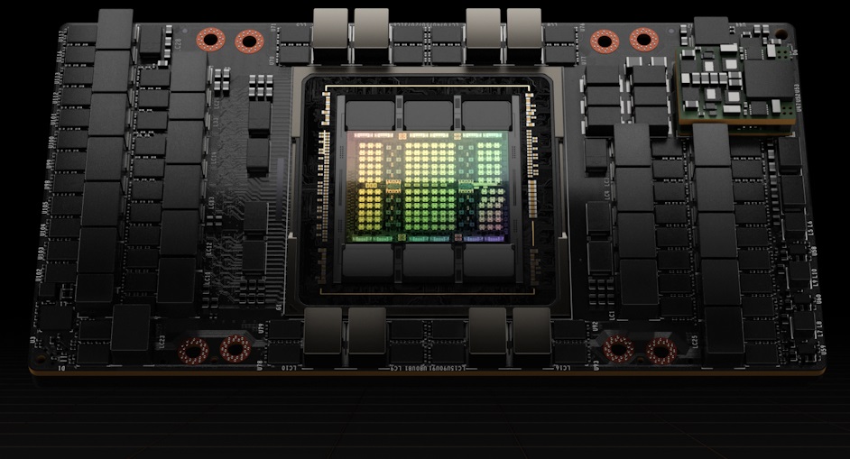
The technical leap represents more than incremental improvement. By doubling the input/output interface width from 1,024 to 2,048 bits—the first such expansion since the transition from HBM1 to HBM2—SK Hynix has fundamentally rewired the economics of AI computing. Each memory stack can now theoretically deliver over 2.5 terabytes per second of bandwidth while consuming 40% less power per bit than previous generations.
Comparison of bandwidth and features across HBM generations (HBM, HBM2, HBM3, HBM4).
| HBM Generation | Standardization/Release Year | Data Rate per Pin (Gb/s) | Bandwidth per Stack (GB/s) | Max Capacity per Stack (GB) | Interface Width (bits) | Channels |
|---|---|---|---|---|---|---|
| HBM | 2013 | 1.0 | 128 | 4 | 1024 | 8 |
| HBM2 | 2016 | 2.0 | 256 | 8 | 1024 | 8 |
| HBM2E | 2019 | 3.6 | 461 | 16 | 1024 | 8 |
| HBM3 | 2022 | 6.4 | 819 | 24 (up to 64 for 16-Hi stack) | 1024 | 16 |
| HBM3E | 2023 | 9.8 | 1229 | 48 | 1024 | 16 |
| HBM4 | 2025 (Projected) | 8 (Projected) | 1600 (Projected, 1.6 TB/s) | 36-64 (Projected) | 2048 (Projected) | 32 (Projected) |
"This isn't just faster memory; it's a different category of memory architecture," notes one semiconductor analyst familiar with the development. "The width doubling forces every other component in the system—controllers, interposers, power delivery—to be redesigned around SK Hynix's implementation."
The company achieved this breakthrough through what it calls Advanced MR-MUF packaging technology, a sophisticated process that stacks up to 12 memory dies while managing heat dissipation and structural integrity. Unlike competitors betting on bleeding-edge manufacturing processes, SK Hynix chose the proven 1b-nanometer DRAM node, prioritizing manufacturing yield and reliability over hero performance claims.
Racing Against Silicon Valley's Demand Clock
The timing couldn't be more critical. NVIDIA's next-generation Rubin platform, expected in 2026, is designed around HBM4 specifications. With AI training costs measured in millions of dollars per model and datacenter operators facing spiraling electricity bills, memory efficiency has become the determining factor in artificial intelligence economics.
Samsung, currently sampling HBM4 with plans for 2026 supply, trails SK Hynix by several months—an eternity in the fast-moving AI hardware cycle. Micron, the American memory giant, won't begin serious sampling until Q4 2025, effectively conceding the early market to its Asian competitors.
Industry sources suggest SK Hynix's technical lead runs deeper than timeline advantage. The company has already delivered working 12-high memory stacks to customers, proving the thermal and mechanical challenges of extreme memory density can be solved at production scale. Competitors remain largely in prototype phases, validating basic functionality rather than demonstrating manufacturing readiness.
The Bottleneck Beyond Memory
Yet even perfect memory chips face infrastructure constraints that could limit near-term impact. TSMC's advanced packaging capacity, essential for assembling complete AI accelerators, remains the industry chokepoint. The foundry's next-generation "Super Carrier" packaging technology, capable of supporting 12 HBM4 stacks per processor, won't qualify until 2027.

This creates an unusual dynamic where memory suppliers must align production with packaging availability rather than pure demand signals. Industry executives privately acknowledge that 2026 will see constrained AI accelerator volumes regardless of memory chip readiness, potentially extending SK Hynix's competitive window.
The constraint also explains why SK Hynix chose conservative manufacturing approaches over aggressive performance targets. With packaging capacity scarce, the premium goes to suppliers who can guarantee yield and reliability rather than those chasing benchmark victories.
CoWoS, or Chip-on-Wafer-on-Substrate, is an advanced packaging technology pioneered by TSMC. It allows for the vertical stacking of chips, enabling greater integration and higher performance compared to traditional side-by-side chip placement.
Investment Implications: Beyond the Memory Cycle
For investors, SK Hynix's HBM4 leadership represents a fundamental shift from cyclical memory dynamics to structural growth. Traditional DRAM markets rise and fall with PC and smartphone cycles, creating predictable boom-bust patterns. AI memory demand follows datacenter capital expenditure cycles—measured in years rather than quarters and driven by technological capability rather than consumer replacement behavior.
The company's approach to customer-specific base dies creates additional competitive moats. Unlike commodity memory that can be easily substituted, HBM4 chips increasingly incorporate custom logic designed for specific AI accelerators. This locks in customer relationships and supports value-based pricing that can persist even as manufacturing costs decline.
Market research suggests HBM demand will grow at roughly 30% annually through 2030, with unit volumes potentially increasing 15-fold by 2035. Unlike previous memory super-cycles driven by temporary imbalances, AI memory demand reflects permanent architectural requirements for machine learning workloads.
Projected global High Bandwidth Memory (HBM) market growth through 2030.
Projected global High Bandwidth Memory (HBM) market growth through 2030.
| Year | Market Size (USD Billion) | CAGR (%) | Source |
|---|---|---|---|
| 2023 | 1.768 | - | |
| 2024 | 2.5 - 2.9 | - | |
| 2025 | 3.0 - 4.03 | 27.3% (from 2024) | |
| 2030 | 9.2 - 85.75 | 24.2% - 68.1% (from 2024/2023) |
The Geopolitical Memory Map
SK Hynix's technical leadership also carries strategic implications as memory becomes central to national AI competitiveness. U.S. export controls on advanced semiconductors have created complex compliance requirements, while Chinese companies seek domestic alternatives to reduce dependence on foreign suppliers.
The company's ability to serve both Western and Eastern markets—while maintaining technological leads over domestic Chinese competitors—positions it to benefit from geographic diversification even as geopolitical tensions escalate. However, this also creates regulatory risks that could constrain customer access or force operational changes.
Industry analysts suggest memory suppliers with proven advanced capabilities may face increasing pressure to align with specific geopolitical blocs, potentially fragmenting the global market. SK Hynix's current technical leadership provides options, but future policy decisions could force difficult strategic choices.
What the Money Should Watch
Investors tracking HBM4's commercial trajectory should focus on three critical metrics: packaging-constrained revenue conversion, speed-bin mix achievement, and customer concentration risks. The percentage of production shipped at full 10+ gigabit speeds will indicate whether SK Hynix's performance claims translate to manufacturing reality.
CoWoS packaging capacity reservations by major customers provide leading indicators of 2026 revenue potential, while progress on 12-high stack yields determines profit margin sustainability. Any diversification beyond NVIDIA as the dominant customer would reduce concentration risk and demonstrate broader market acceptance.
The broader investment thesis rests on AI infrastructure spending maintaining current growth trajectories. Should model training costs plateau or energy constraints force datacenter construction delays, even superior memory technology faces demand headwinds that could pressure pricing and utilization rates.
Nevertheless, current evidence suggests SK Hynix has engineered the memory solution AI desperately needs—precisely when the industry can pay premium prices for performance and reliability. In the high-stakes race to power artificial intelligence, timing may prove as valuable as technology itself.
House Investment Thesis
| Category | Summary & Key Points | Quality/Moat Assessment | Timing | Risks & Mitigators |
|---|---|---|---|---|
| Executive Take | HBM4 development complete; mass-production line ready. 12-high stacks sampled March 2025. Key innovation is 2,048-bit I/O (vs. 1,024-bit), doubling bus width and raising switching costs. >10 Gb/s/pin & >40% power-efficiency gain targets AI memory wall. No near-term substitute. | Execution leadership. Moat from width doubling and customer lock-in. Secures >55% share likelihood for SK hynix through 2026. | 2026 is the revenue inflection year for HBM4. 2025 is validation/low-volume pre-build. | Packaging capacity (interposer/substrate), not die output, is the primary constraint. |
| What's New | 2,048-bit bus & >10 Gb/s/pin (~2.0–2.56 TB/s per stack). Uses 1b-nm DRAM + Advanced MR-MUF for better yields/thermals. Custom base dies for key customers (e.g., NVIDIA) increase switching friction. | Pragmatic process/package focus on "ship-ability." Customization creates a moat and supports value-based pricing. | Custom base dies lock in lead customers for the medium term. | Competitors developing their own custom solutions. |
| Market & Economics | HBM demand CAGR ~30% to 2030. 2026 accelerators (NVIDIA Rubin) to use HBM4. ASP and gross margins stay elevated due to value pricing, but capex/COGS rise. Supply discipline from packaging constraints reduces price-war risk. | HBM4 GM% expected to be > HBM3E GM% for SK hynix. HBM3E oversupply has limited read-through to HBM4 scarcity. | TSMC's 9-reticle "Super Carrier" for 12 HBM4 stacks not qualified until 2027, capping extreme topologies until then. | Packaging bottleneck (CoWoS, substrate supply) is a cap on near-term upside. |
| Competitive Scorecard | SK hynix: #1 in share & reliability. First to dev-complete & MP-ready. Samsung: Credible #2; HBM4 samples out; plans 2026 supply; improving yields. Micron: Shipping samples; selective sockets; third supplier unless major win. | SK hynix has best-in-class packaging and NVIDIA entrenchment. Samsung is closing the gap. Micron is competitive on perf/W but #3. | 2026 supply plans confirmed by all. Race is for first-wave 2026 accelerator shipments and speed-bin stability. | Samsung/Micron catching up on yield/thermals faster than expected could claw back share. |
| Key Risks | 1. System-level closure: PHY timing, thermals may force lower speed bins. Mitigator: Controller IP (e.g., Rambus) validated up to 10 Gb/s. 2. Packaging throughput/yield: TSMC CoWoS is a chokepoint. 3. Geopolitics: U.S. export controls on China. 4. Competitor catch-up. | Risks are underpinned by technical and supply chain constraints, not product viability. | Risks primarily affect the 1H'26 ramp timeline and speed-bin mix. | |
| Bearish Toggles | Change in thesis if: 12-Hi reliability issues force speed derates; 2026 accelerators choose mixed HBM3E/HBM4 configs due to packaging scarcity; competitor lands a lead socket before SK hynix hits stable 10 Gb/s bins. | These events would indicate a failure of technical execution or a shift in the competitive landscape. | Would delay the 2026 HBM4 revenue inflection and mix shift. | |
| Positioning & KPIs | SK hynix longs: Confirmation of durable moat and 2026 earnings up-leg. Track speed-bin mix/yield and packaging-constrained revenue. Peers: Must demonstrate 10 Gb/s stability by mid-2026 to avoid being price-takers. | KPIs: % of MP at ≥10 Gb/s; 12-Hi yield; CoWoS reserved capacity; share of custom base die shipments; lead customer acceptance reports. | Key timing for validation: first-silicon bring-up for 2026 chips (Rubin). | |
| Bottom Line | Excellent engineering and commercially decisive. Width doubling + >10 Gb/s + proven packaging + NVIDIA relationship should keep SK hynix in the lead through 2026. Primary cap is packaging capacity, not device readiness. | Underwrites continued share leadership and margin outperformance in HBM. | Validation/yield surprises could dent the 1H'26 ramp. |
Investment decisions should consider individual risk tolerance and professional financial guidance. Past performance of technology stocks does not guarantee future results.